 Inglés UdeA - Cabezote - WCV(JSR 286)
Acciones
Inglés UdeA - EnlaceInteres - JSR(286)
Acciones


Signpost
Acciones
Generales
UdeA boots up powerful electron microscope
Acciones
UdeA boots up powerful electron microscope
A new transmission electron microscope (TEM), one of the most advanced technologies to study matter, is now available to UdeA’s scientific community as well as academic and industrial partners nationwide.
While science and technology focus on increasingly smaller areas such as nanotechnology and tissue engineering, there is a growing demand for specialized technology for the study of microstructures.
Conventional optical microscopes use visible light to illuminate objects of interest. The light (photons) emitted from the light source – usually a halogen lamp – is used to examine the sample, showing the resulting image directly on a computer screen.
However, due to the wavelength and other characteristics of light and the human visual system, this type of technology is limited by the sample size. In 1931, the German physicist Ernst Ruska managed to develop a device that allowed him to replace photon-based radiation sources by using electron-based radiation since electrons can also behave as both a wave and a particle but with much more energy. Ruska, as well as other engineers and physicists, made major contributions to the development of electron optics.
Unlike TEMs, scanning electron microscopes (SEMs) produce images of a sample by scanning it with a beam of electrons producing various signals that can be detected through a series of sensors which provide information about the sample's surface topography based on its physical and chemical characteristics.
On the other hand, TEMs give researchers the ability to carry out mapping of both the external and internal surfaces of the sample thus providing genuine atomic resolution, which requires much more energy so that the electron beam can pass through the sample in order to reveal more detailed images.
“In general, sample preparation for a scanning electron microscope is much simpler than in the case of TEMs as the latter requires the use of very thin slices of the sample so that the electron beam can pass through it,” says professor Félix Echeverría, coordinator of UdeA’s Center for Materials Research and Innovation (CIDEMAT). “TEMs also have much more energy than conventional microscopes, which results in higher resolution images,” he added.
Transmission electron microscopes boast state-of-the-art features widely used by scientists and engineers around the world, including Nobel laureates, such as the possibility to carry out ultrahigh-resolution crystallographic calculations, which in other words means that one may be able to view and analyze small materials such as nanoparticles and explore its crystalline structure,” the researcher said.
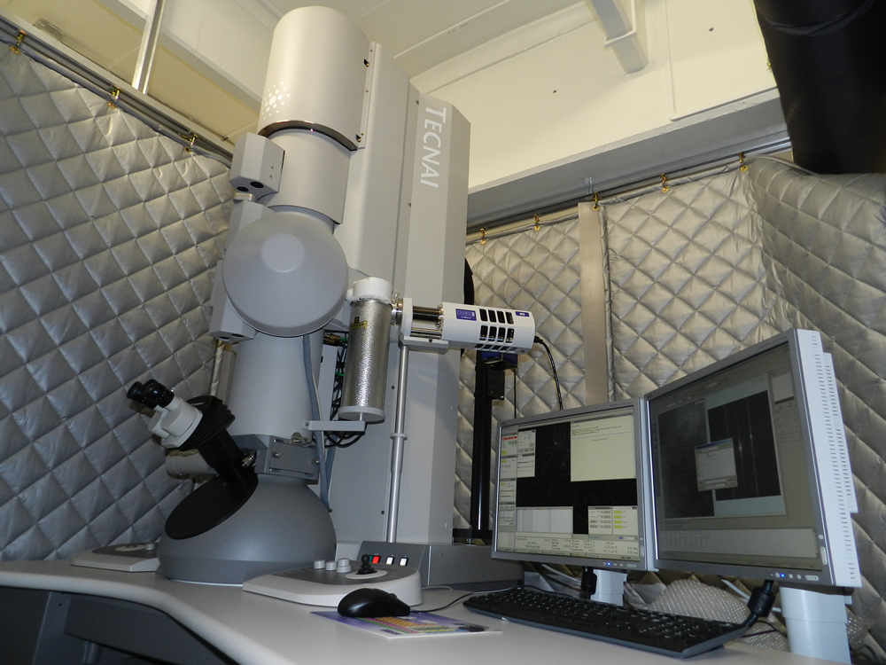
UdeA’s TEM
The FEI Tecnai G2 F20 is equipped with a state-of-the-art sample preparation system and combines a wide range of analysis techniques of both the TEM and SEM, which is known as S/TEM.
Although the University Research Center (SIU) is equipped with a modern scanning electron microscope, factors such as the boom in nanotechnology encouraged the University to acquire a transmission electron microscope to meet the stringent demands of its scientific community, says professor Echeverría.
While SEMs are used to observe the larger areas of a sample, transmission electron microscopes have a greater resolving power that allows it to see much smaller objects in finer detail due to the electron beam. When combined, these two technologies provide high-definition images of a larger area allowing the researcher to perform comprehensive, high-level explorations.
UdeA’s new TEM is equipped with a field emission gun and has an accelerating voltage of 20-200 kV, which allows performing high-resolution analysis of a wide range of materials.
Who will benefit from the new TEM?
TEMs are undoubtedly a useful tool for a variety of research groups and disciplines and to explore biological materials such as tissues and cells, among others.
Transmission electron microscopes have been widely used to study the physical and chemical properties of materials, including its morphology and crystalline structure. “By using a type of specialized probes it is possible to determine the chemical composition of a specific material as well as its shape and size at resolutions as high as the angstrom-scale resolution level,” professor Echeverría said.
The acquisition of the 1.5 million dollar TEM involved the participation of various departments across the University. The new equipment was purchased with funding from UdeA’s Research and Development Committee (CODI), the Office of Graduate Studies and the various research groups at Universidad de Antioquia.
This state-of-the-art equipment is now available for use by the country’s scientific community. The TEM is operated by a highly skilled team of experts at the University Research Center (SIU) in order to provide researchers with high-quality images and services.
If you have any questions or would like more information about this service, please contact Professor Félix Echeverría. He can be reached by phone at 574-2196615, or via email at felix.echeverria@udea.edu.co. You can also contact the University Research Center (SIU) by phone at 574-2196416 or at comunicacionessiu@udea.edu.co
Portal U de A - Redes Sociales - WCV(JSR 286)
Acciones
Inglés UdeA - Iconos Footer - WCV(JSR 286)
Acciones